Quickdev2 Progress
After building the quickdev16 in the summer of 2010 we decided to work on
a 2nd version off the quickdev16, which we called quickdev2. All this work was done in the summer of 2010 but i never got around
to finish the project nor to blog about it. So here is a little overview:
The next quickdev should be a little bit faster and should have more features.
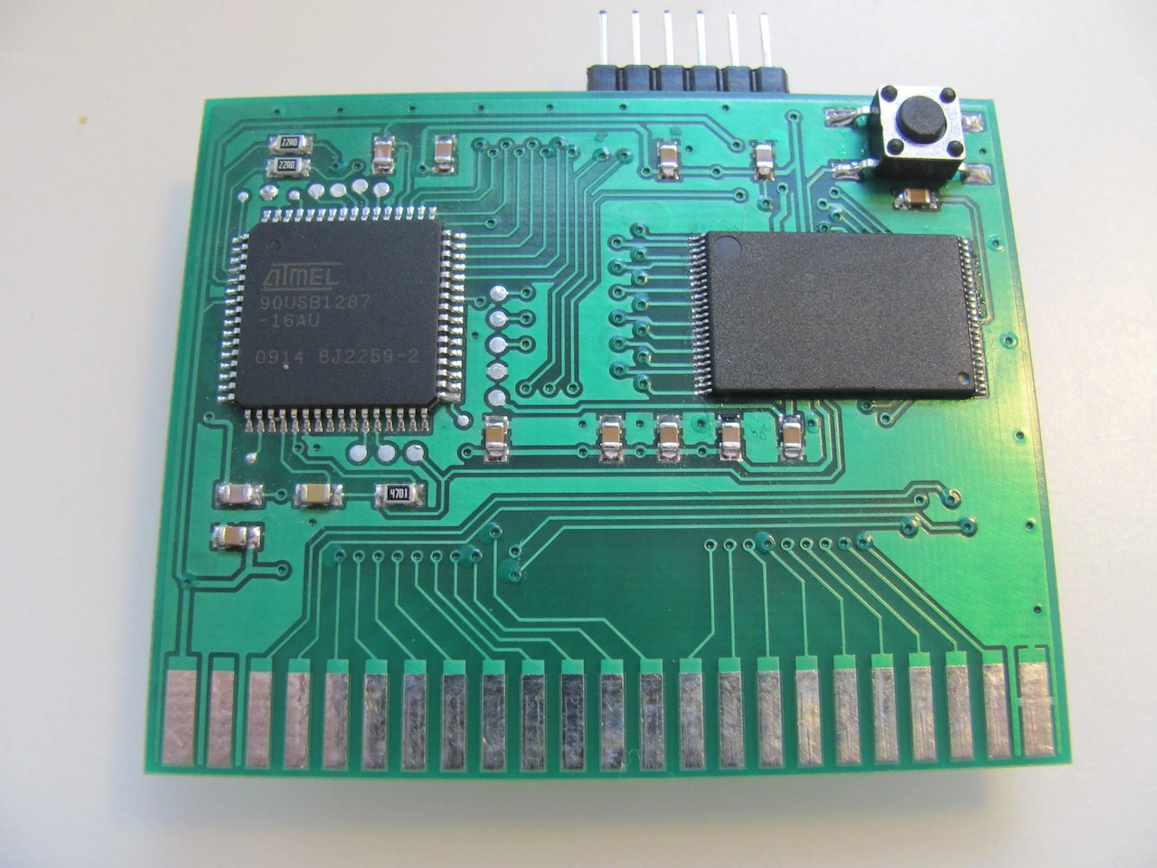
So we selected a new CPU, the Atmel at90usb1287 that can handle USB via hardware and has more SRAM. To simplify the logic part we opted for a XILINX CPLD xc95144xl.
We used a bigger Cypress 16-Mbit SRAM CY62167E.
The AVR would expose the USB interface to the PC side, as a masstorage device using the LUFA library. The
AVR has a data bus to the CPLD. The CPLD is also connected to the external SRAM.
In the CPLD we implemented a SREG, counter, commandmuxer and memory interface in Verilog.
The system top looks like this:
module system (

    inout [7:0] sram_data,
    output [20:0] sram_addr,
    output sram_oe_n,
    output sram_we_n,
    output sram_ce_n,


    output [7:0] snes_data,
    input [20:0] snes_addr,

    inout [7:0] avr_data,
    input [7:0] avr_ctrl,
    input avr_clk,
    output [7:0] debug
);
We have a 8 bit data bus and 21 bit address bus to the SRAM. 3 extra lines for OE,WE and CE.
Then there is the same setup for the SNES side. 8 Data and 21 address line. No more control lines to
the SNES are currently implemented. There is a 8 bit data and 8 bit control bus to the AVR.
Finally we have a CLK line from the AVR to the CPLD and a 8bit debug bus.
The AVR clocks its own clock into the CPLD, which is feed into a DCM and is divided by 2.
This clock signal is feed into the FSM and SREG internally.
The avr_ctrl bus is feed into a commandmuxer which
drives the other components on the CPLD. Foremost it drives a FSM which manages the
data routing between AVR <-> SRAM and SRAM <-> SNES.
module bus_fsm #(
    parameter DWIDTH = 8
)(
    input                   clk,
    input                   reset,
    input                   we_n,
    input                   oe_n,
    inout   [DWIDTH-1:0]    avr,
    inout   [DWIDTH-1:0]    sram,
    inout   [7:0]           debug
);

parameter SIZE   =  3;
parameter IDLE    = 3'b000;
parameter WE      = 3'b001;
parameter BUFAVR  = 3'b010;
parameter BUFSRAM = 3'b011;
parameter OE      = 3'b100;


reg   [SIZE-1:0]          state;
reg   [SIZE-1:0]          next_state;
reg   [DWIDTH-1:0]        buffer_avr;
reg   [DWIDTH-1:0]        buffer_sram;
reg   [DWIDTH-1:0]        buffer;

assign avr = buffer_avr;
assign sram = buffer_sram;

always @ (state or we_n or oe_n)
begin : FSM_COMBO
    next_state = 3'b000;
    case(state)
    IDLE : if (we_n == 1'b0) begin
            next_state = BUFAVR;
        end else if (oe_n == 1'b0) begin
            next_state= BUFSRAM;
        end else begin
            next_state = IDLE;
        end
    BUFAVR: if (we_n == 1'b0) begin
            next_state = WE;
        end else begin
            next_state = IDLE;
        end
    BUFSRAM: if (oe_n == 1'b0) begin
            next_state = OE;
        end else begin
            next_state = IDLE;
        end
    OE : if (oe_n == 1'b0) begin
            next_state = BUFSRAM;
        end else begin
            next_state = IDLE;
        end
    WE : if (we_n == 1'b0) begin
            next_state = BUFAVR;
        end else begin
            next_state = IDLE;
        end
  endcase
end

//----------Seq Logic-----------------------------
always @ (posedge clk)
begin : FSM_SEQ
    if (reset == 1'b1) begin
        state <= #1 IDLE;
    end else begin
        state <= #1 next_state;
  end
end

//----------Output Logic-----------------------------
always @ (state)
begin : OUTPUT_LOGIC
  case(state)
    IDLE: begin
        buffer_avr <= 8'bz;
        buffer_sram <= 8'bz;
        buffer <= 8'bz;
    end
    WE: begin
        buffer_sram <= buffer;
    end
    OE: begin
        buffer_avr <= buffer;
    end
    BUFSRAM : begin
        buffer <= sram;
    end
    BUFAVR : begin
        buffer <= avr;
    end
    default : begin
        buffer_avr <= 8'bz;
        buffer_sram <= 8'bz;
    end
  endcase
end

assign debug = { clk,we_n,oe_n,state,2'bz};
endmodule
From the AVR software side a SRAM write looks like this.
void sreg_set(uint32_t addr)
{


    uint8_t i = 21;
    #if SREG_DEBUG
    uart_putstring("sreg_set\n\r");
    #endif
    SET_AVR_SREG_EN_HI();
    while(i--) {
        if ((addr & ( 1L << i))){
            SET_AVR_SI_HI();
    #if SREG_DEBUG
            uart_putchar('1');
    #endif
        } else {
            SET_AVR_SI_LO();
    #if SREG_DEBUG
            uart_putchar('0');
    #endif
        }
        SET_AVR_SREG_EN_LO();
        SET_AVR_SREG_EN_HI();
    }
    #if SREG_DEBUG
    uart_putstring("\n\r");
    #endif
}

void SRAM_write(uint32_t addr, uint8_t data)
{

    // set direction of data port
    AVR_DATA_DIR = 0xff;
    // load address
    sreg_set(addr);
    // disable OE and WE
    SET_AVR_OE_HI();
    SET_AVR_WE_HI();
    // wait for FSM to go into IDLE state
    nop();
    nop();
    // write data
    AVR_DATA = data;
    // enable WE
    SET_AVR_WE_LO();
    // wait for FSM to go into WE state
    nop();
    nop();
    nop();
    nop();
    // disable WE
    SET_AVR_WE_HI();
}
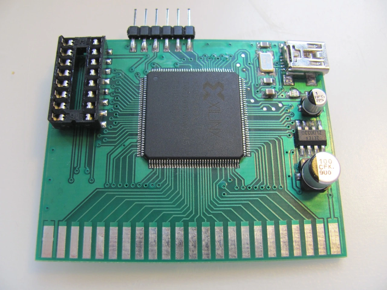
The development was done on our new prototype board, which Max layouted for us.
I used an AVR Dragon for the AVR programming part and debugging via JTAG. For the CPLD side i used a homebrew Xilinx Platform cable alongside with ISE. I quickly stopped using the IDE and just cooked my own Makefile using the Xilinx commandline tools.
Most of the logic was developed using a testbench and running through iverilog.
But having a module working in a testbench doesn't mean that it works on real hardware.
We had todo a lot of debugging on the real hardware. This involved a lot
of test probe soldering. Luckily we had my 8bit Saleae LA which helped a lot to
track done some Problems. But the biggest issue was to get the timing right with the FSM for the memory bus.
We hacked this in a 3 day weekend sprint and implemented the SRAM read and write from the AVR side.
But then we hit a wall and didn't implement the SNES side. The project lost some traction.
Max had moved to Berlin we couldn't work together on the project anymore. We lost a little interest because the
sd2snes project achieved what we we intended to do and Ikari_01 did far better job then we did.
I recently got word the sd2snes is considered stable and a first batch is sold.
We plan to start working on this again. To implement the SNES side of the memory we would need to increase the speed
of the FSM to get it into IDLE state and then in SNES state within 120ns or 200ns after the SNES does a CS on the cartridge.
Since the AVR drives the CPLD clock with 20MHz, we would need some kind of PPL to run the FSM with like 60MHz, which should
be plenty to run the FSM for the SNES SRAM read.
We appreciate any comment or suggestion for the hardware design of this project.
Quickdev2 Progress Read More »