Bildschirmtext (BTX)
Being a kid from the 80ies, i never came around using the german Bildschirmtext service. Luckily I found a recent implementation of the BTX protocol with some pages from the late 80ies and early 90ies.
Run the BTX server
brew install socat
git clone https://github.com/bildschirmtext/bildschirmtext
cd bildschirmtext
python3 -m virtualenv env
source env/bin/activate
pip install -r requirements.txt
cd server
socat TCP-LISTEN:20000,reuseaddr,fork 'exec:python neu-ulm.py'
Compile and run the client
brew install sdl2
git clone https://github.com/optixx/btx_decoder
cd btx_decoder/sdl
make
./btx_sdl 127.0.0.1:20000
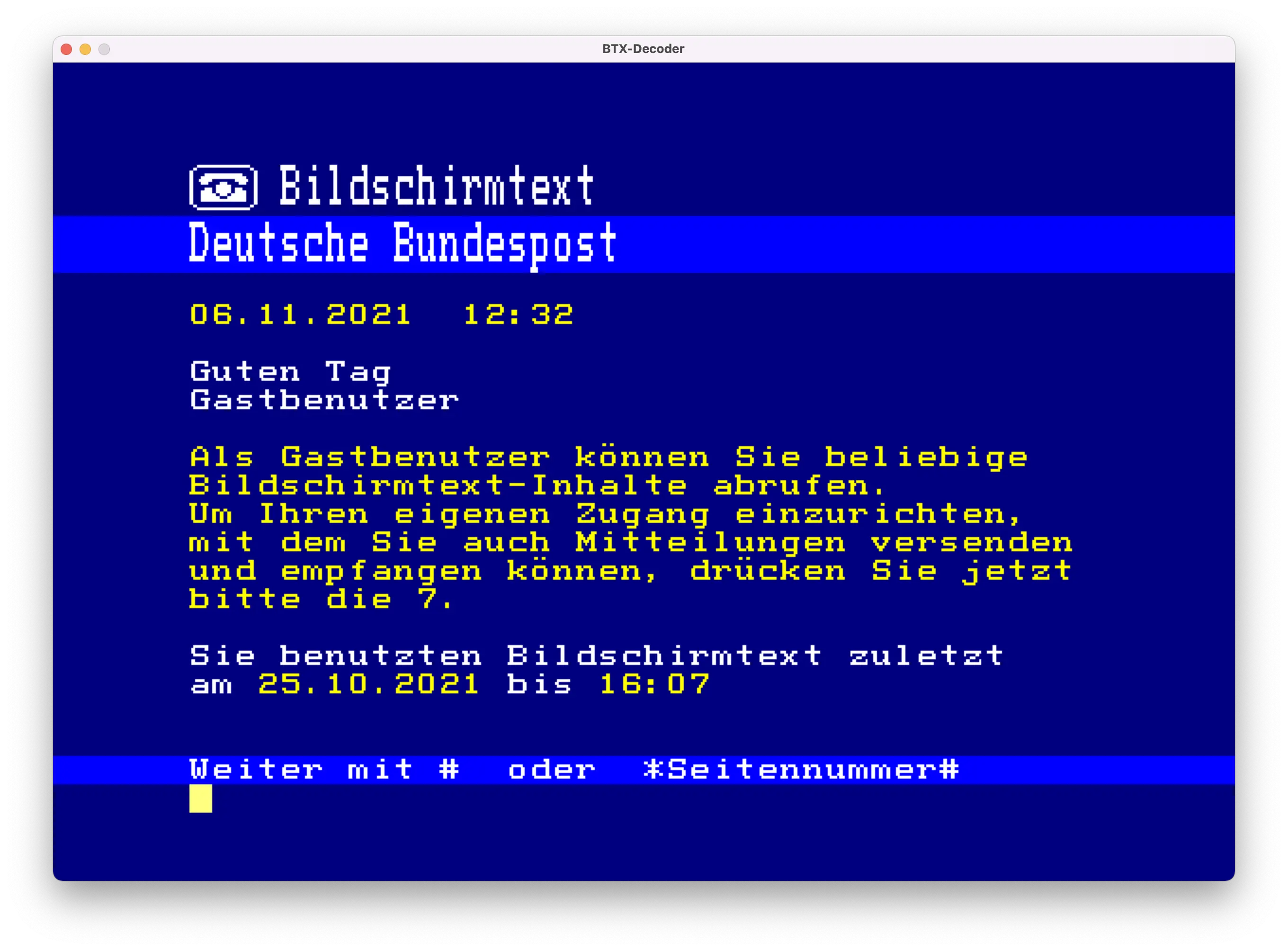
Usage
The guest user (user 0, co-user 1) has an empty password, so you can log in as a guest by pressing “#” 3x at startup (or DCT once). You can define your own users by creating files in users/ and secrets/.
*00#: Retransmit page (in case of transmission errors)
*09#: create page again (or reload from database)
*#: return to the previous page
*page number#: navigation to a specific page
[0-9] and #: navigation to a following page
**: deletes the input
*9#: logs off the user
Bildschirmtext (BTX) Read More »